Objective: fewer losses, higher efficiency
However, a way out is in sight: the material silicon carbide could be perfectly suited for the construction of modern high-performance transformers – at least theoretically. This is because the chemical compound comprising silicon and carbon has only been available in a sufficient quality for research for a few years. It possesses semiconductor properties that are much better suited than other materials for use in the electricity grid. For example, the power losses experienced when switching voltages are up to two orders of magnitude lower than is the case with traditionally used silicon.
As silicon carbide is still so new, however, the design of suitable structures for the components has only been researched for relatively low power outputs and not for components with switching capacities in the megawatt range, as will be the case in the real electricity grid.
As part of the joint project “Swiss Transformer”, an interdisciplinary team led by Jens Gobrecht at the Paul Scherrer Institute has therefore focused its attention on the optimisation of precisely this output: where the silicon carbide comes into contact with the oxide layer of the power electronic components. In computer experiments, the team simulated how different construction methods would behave under high switching capacities.
In addition to these models, the team also closely examined the surface properties of silicon-carbide-based components. As these innovative transformers are not yet industrially manufactured, it is important to anticipate, understand and solve potential problems in serial production. One finding is that the surface of the silicon carbide has different properties to that of conventional materials, which influences the manufacturing process: while the oxidation of silicon produces a very smooth interface between the silicon and the oxide, the oxidation of silicon carbide produces a very rough interface. This has a negative effect on the resistance of the component when it is switched on. Through the use of synchrotron radiation at the PSI, the researchers worked on scientifically clarifying the formation of this roughness in the nanometre range. Only then is it possible to modify the manufacturing process in such a way that the rough surface is not created in the first place.
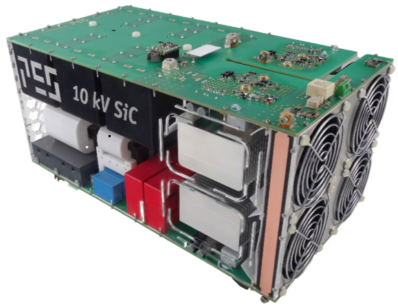
The project thus makes an important contribution to the joint project “Swiss Transformer”. The smart grid of the future – and thus the achievement of the ambitious goals of Energy Strategy 2050 – will only become possible through efficient components that can withstand the loads of the grid.


